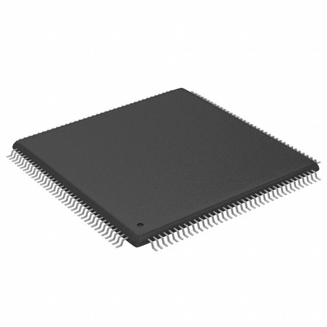
Xilinx XC3S200-4TQG144C FPGA Chip Introduction
Creation Date
By Lzchips
The XC3S200-4TQG144C is a field-programmable gate array (FPGA) chip produced by Xilinx, offering high flexibility and programmability. Utilizing advanced CMOS technology, this chip combines high performance, low power consumption, and abundant resources suitable for various applications, including communications, image processing, and embedded systems.

Key Features:
Capacity: The XC3S200-4TQG144C chip features 200,000 system logic cells, providing ample resources for implementing complex logic functions and algorithms.
Operating Frequency: Supports operating frequencies of up to 400MHz, meeting the demands of high-performance and real-time applications.
Abundant Resources: Offers plentiful memory resources, including distributed RAM, block RAM, and register resources, effectively supporting data processing and storage requirements.
General I/O: Provides a large number of general-purpose input/output pins, supporting connectivity and communication with various external devices.
Low Power Design: Utilizes advanced low-power CMOS technology, delivering excellent power efficiency suitable for applications with stringent power requirements.
Application Areas:
The XC3S200-4TQG144C FPGA chip is suitable for a wide range of application areas, including but not limited to:
Communication systems Image processing Smart control Embedded systems Data acquisition and processing
Usage Procedure:
Step 1: Design and Development
Requirement Analysis: Determine system functionality and performance requirements based on application needs.
Logic Design: Write logic designs using hardware description languages like VHDL or Verilog, defining the functionality and interfaces of various modules.
Simulation Verification: Verify the design through simulation tools to ensure correct and stable logic functionality.
Step 2: Synthesis and Implementation
Synthesis and Optimization: Utilize development tools like Xilinx ISE or Vivado to synthesize and optimize the design, generating synthesized logic netlists.
Place and Route: Perform place and route operations to map the logic netlist onto the physical resources of the XC3S200-4TQG144C chip and achieve timing optimization.
Generate Bitstream: Generate bitstream files containing configuration information for programming the FPGA chip.
Step 3: Loading and Debugging
Download Bitstream: Load the bitstream file into the target chip through JTAG interface or other download methods.
Functional Verification: Verify the functionality of the design loaded into the chip to ensure it meets expected requirements.
Debugging and Optimization: If necessary, debug and optimize the design to meet actual application needs.
Step 4: Integration and Deployment
System Integration: Integrate the FPGA chip into the target system, establishing interfaces and communication with other hardware and software modules.
Deploy Application: Deploy the configured system in practical scenarios and conduct functionality verification and performance testing.
Step 5: Maintenance and Updates
System Maintenance: Regularly maintain and inspect the system to ensure its stable operation.
Function Updates: Update and optimize system functionality as per requirements to keep it up-to-date.
Following this procedure, you can successfully design, develop, and deploy applications based on the XC3S200-4TQG144C FPGA chip, implementing various complex logic functions and algorithms to meet diverse domain requirements.